Figure
1. Formation of Schottky
barrier of metal to n-type semiconductor.
the metal into the semiconductor
conduction band is
qjBn = q(jm
- c). (1)
For
contact between a metal and a p-type semiconductor with jm < js, the barrier
height qjBp is given
by
qjBp
= Eg - q(jm
- c), (2)
where Eg is the bandgap. Figure 2
gives a Schottky barrier formed by contacting an
metal with an p-type semiconductor when jm
< js in an
ideal case The two other cases of ideal
metal-semiconductor contacts (jm < js
for n-type and jm > js for p-type semiconductors) result in ohmic contacts characterized with an linear current-voltage
curves. Conclusions derived from the
ideal metal-semiconductor contacts are referred to Schottky-Mott
rule.
Ideally,
the barrier height depends only on the metal work function and on the
semiconductor bandgap and electron affinity. In practice, however, it is
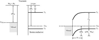
(a) Band
diagrams for the metal and (b)
Equilibrium band diagram for
the
semiconductor before joining the junction
Figure
2. Formation of Schottky barrier of metal to p-type
semiconductor.
difficult to alter the barrier
height by using metals of the varying work function. It is experimentally observed that the
barrier height for the common semiconductor materials Ge, Si, GaAs, and other III-V materials is relatively independent
of the work function of the metal. A Schottky
contact is generally formed on both n-type and p-type semiconductors with jB » Eg/3
for both cases. The relative constancy of
the barrier height with work function of metals is sometimes called Fermi level
pinning, referring to the fact that the Fermi level in the semiconductor is
pinned at some energy in the band gap to create a Schottky
contact3,4. J. Pelletier et
al.5 reported Fermi level pinning in 6H-SiC attributed to intrinsic
surface states, suggesting little dependence of barrier height on the work
function of the metal. L.M. Porter et
al.6 found that the barrier height differences of Ti, Pt, and Hf contacts to n-type (0001) 6H-SiC were all within a few
tenths of 1 eV, giving evidence that the Fermi level
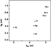
(a) Barrier height vs. work function for 3C-SiC

(b) Barrier height vs. work
function for 6H-SiC
Figure 3. Schottky barrier height jB of various metal contacts to
SiC versus metal work function jm (after J.R. Waldrop et al.7,8)
is pinned in the bandgap. On the
other hand, J.R. Waldrop et al.7,8 reported a strong dependence of
barrier height for metal contacts to 3C- and 6H-SiC on the work function of the
metal. Figure 3 (a) and (b) show the Schottky barrier height jB
plotted against the respective metal work function jm
for 3C- and 6H-SiC, respectively. The
details of Schottky barrier formation are not yet
fully understood. It appears, however,
that interfacial electronic states due to defects, metal induced gap states,
and interfacial chemistry play important roles during contact formation.
4. Carrier Transport processes
The
carrier transport mechanisms through the metal-semiconductor interface are
strongly influenced by the donor concentration in the semiconductor and the
temperature. Three typical cases are
schematically shown in Figure 4 for a n-type semiconductor. Figure 4(a) depicts the situation where a
semiconductor is lightly doped (Nd < 1017/cm3). In this case, the depletion width W is wide and the electrons cannot
tunnel through the interface. The only
way for the electron to transport between the metal and the semiconductor is by
thermionic emission (TE) over the potential barrier jBn. Figure 4(b) shows the band diagram of a metal
contacting a semiconductor doped at an intermediate level (Nd = 1017
to 1018/cm3). In
this case, the electrons can partially tunnel through the interface and both
thermionic and tunneling process are important, which is referred to
thermionic-field-emission (TFE). When
the semiconductor is extremely heavily doped ( Nd > 1018/cm3), the
electrons can tunnel through from the Fermi level in the metal into the
semiconductor. This process is called
field-emission (FE), which is shown in Figure 4(c).
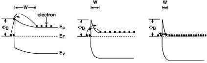
(a)
Low ND;
(b) Intermediate ND; (c)
High ND.
Figure
4. Conduction mechanisms through metal/n-type semiconductor interface with different doping levels.
A
useful parameter indicating the electron tunneling probability is kT/E00, where E00 is a characteristic
energy defined by
E00
= 
 (3)
(3)
where h is Planck’s constant, h,
divided by 2p,
m* is the effective mass of the
tunneling electron, e
is the dielectric constant of the semiconductor. With increasing doping concentration Nd, the width of the depletion region W decreases, making it easier for
carriers to tunnel through. This
indicates that when E00 is
high relative to thermal energy kT, the probability of electron transport by tunneling
increases. Therefore, the ratio kT/E00 is a useful measure of
the relative importance of the thermionic process to the tunneling
process. For lightly doped
semiconductors, kT/E00 >> 1 and
thermionic emission is the dominant current flow mechanism. For kT/E00 » 1,
both thermionic and tunneling mechanisms are dominant, and for kT/E00
<< 1, the tunneling mechanism dominants the carrier transport mechanism9.
5 SiC
metallization process and characterization
The
metallization procedures for SiC are basically the
same as those used for Si and GaAs techniques. Some highlights of metallization process and
characterization are briefly given as follows.
Wafer
surface preparation The
preparation of the SiC wafer surface prior to metal
deposition is a very important step for metallization. Surface contamination can reduce adhesion of
metals to SiC and increase contact resistance. Any contaminants and native oxide layer on
the wafer surface must be removed before metal deposition. Solvents, such as trichloroethylene (TCE), trichloroethane (TCA), acetone, methanol, and propanol are used to degrease SiC
wafer. In order to obtain a fresh SiC surface free of oxide, A. Evwaraye
at al.10 and M.I. Chaudhry et al.11
suggested to grow thermal oxide and subsequently remove it by acid
etching. This procedure also removed
defects on SiC surface caused by mechanical
polishing. Various acids and bases are
used to etch SiC wafer surface, such as HF, H2SO4, HCl, NH4OH:H2O2:H2O,
HCl:H2O2:H2O, H2SO4:H2O2,
HNO3:H2SO4:H2O, K2CO3,
and KOH melt. Prior to metal deposition,
in-situ surface cleaning is also utilized in which sputter etching or
irradiation of high-energy laser beam is commonly performed.
Metal
deposition techniques The most
common techniques used for metal deposition include sputtering, evaporation,
chemical vapor deposition (CVD), and molecular-bean epitaxy (MBE). Sputtering is a well-established deposition
technique for metallization. It is based
on the bombardment of a target with energetic ions, which knock off surface
atoms by energy transfer. These released
atoms land on the wafers to become part of the film coating.
In
evaporation techniques, the deposition material is vaporized in a vacuum from
its liquid phase, and the vapor is then transported and deposited onto the
wafer. The vacuum used for evaporation
is higher than 10-3 torr. At this low
pressure, the residual gas molecules have a mean free path of the order of 1
m. Therefore the evaporated vapor suffers
no collision from the residual gas and is able to achieve a straight-line
travel from the target to the surface of the wafer. The condensation of the vapor on the wafer is
achieved through a nucleation and growth process.
Chemical
vapor deposition (CVD) has been used as a deposition technique for many years
and for a wide variety of end users. Its
use in electronics is widespread as well.
CVD uses volatile compounds containing the deposition species as
transport agents, with these agents being chemically reacted on the
semiconductor surface, creating the desired deposit and other chemical species
as the reaction product. Excellent step
coverage and selectivity are two major advantages that CVD has and make it
unique and very attractive as a deposition technique.
A
new approach to metal deposition is provided by the molecular-beam epitaxy
techniques (MBE). In this method, a beam
made of atoms of the material to be deposited is directed at the semiconductor
substrates. The incidence rate on the surface
is usually low in order to allow the atoms to rearrange themselves on the
surface in structured layers according to their particular lattice structure in
the bulk form. For the same reason, the
substrate is usually kept at an elevated temperature to assist migration of the
impinging atoms. A successful MBE growth
requires an absolutely clean substrate surface.
This means that an extremely high vacuum is required to minimize surface
contamination that would interfere in the formation of a smooth transfer of the
crystalline structure at the interface.12,13
Annealing With a few exceptions, metal contacts on SiC usually illustrate rectifying characteristics. Annealing is often required to form ohmic contacts with low contact resistivity and good thermal
stability. Since the annealing time
required for contacts to SiC is generally longer than
contacts to, for example, GaAs, traditional annealing
is more often used than rapidly thermal annealing (RTA). Annealing is usually performed in an
atmosphere of Ar, vacuum or forming gas (3%H2
in N2). Depending on contact
systems, the annealing temperatures are ranging from 300° to 1200°C, and the
annealing time varies from a few seconds to a few hours. During annealing, silicides and/or carbides are usually formed that may play
a role of decreasing the Schottky barrier height and
hence the contact resistance.
Characterization In
metal-semiconductor contacts a critical quantity which describes the
relationship between the two materials is the Schottky
barrier height, jB. In general, Schottky
barrier height is also a property which best indicates the electrical
characteristics of the contact. Schottky barrier height can be determined by several
different techniques, such as current-voltage measurements, capacitance-voltage
measurements, and x-ray photoelectron spectroscopy.14,15 The most important parameter describing an ohmic contact is its specific contact resistance or contact
resistivity rc. There are different methods to measure
contact resistivity. Among them, the
transmission line measurement (TLM)16,17 is a popular
technique. In TLM, the contact
resistivity is given by
rc. = Rc2
z2 / rs
=  z
Lt (4)
z
Lt (4)
where Rc is the contact
resistance, R0 is the
total resistance at zero distance and Rc = R0/2,
z is the width of the TLM pad, rs
is the semiconductor sheet resistance, and Lt is the transfer
length. Other common methods used for
contact resistivity determination includes the circular transmission line
method18 and the four
point probe method19,20.
In
order to study the interface reaction and to identify compounds formed during
annealing, Auger electron spectroscopy (AES), transmission electron microscopy,
Rutherford backscattering spectrometry (RBS), and x-ray diffraction (XRD) are
techniques often employed. A concise
description on these analyzing techniques can be found in ref. 21.
6. Schottky
contacts on SiC
Many
metals form Schottky contacts on SiC
in the as-deposited condition. In order
to obtain good Schottky contacts, suitable metals
must possess large barrier height jB
with SiC. If Schottky-Mott rule applies, this means the metals must have
high work function for contacts to n-type SiC or low
work function for contacts to p-type SiC. Another important consideration is the high
temperature stability of the contacts.
At elevated temperatures, metals react with SiC
to form silicides and/or carbides, which may increase
or decrease the Schottky barrier height.
The
formation of Schottky barrier contacts to n-type
3C-SiC (100) for Pd, Au, Co, Ti, Ag, Tb, Al was investigated by J.R. Waldrop
and et al.7 These metal
contacts exhibited a wide range of jB,
0.16-0.95 eV; within this range an individual contact
jB, value
depended strongly on the metal work function in general accord with the Schottky-Mott limit.
J.R. Waldrop et al.8,22 also systematically studied the
formation of Schottky barrier contacts to n-type
6H-SiC for Pd, Au, Ag, Tb, Er, Mn, Al, and Mg.
The jB values
for these metal were found to extend over a wide 1.3 eV
range. It was also discovered that to a
varying degree jB depended
on the 6H-SiC crystal faces and the interface chemical reactivity and changes
in jB that
occur for annealed metal contacts were also crystal face dependent with the
C-face to be significantly more reactive than the Si-face. Schottky barrier
values of above metals are listed in Table 1.
Au
forms Schottky contact to SiC
with a high barrier height. S. Yoshida
et al.23 produced good quality Schottky
barrier contacts by evaporating Au onto chemically etched surfaces of n-type
3C-SiC epilayers grown by CVD, and obtained the
barrier height of 1.15±0.15 eV and 1.11±0.03 eV by the capacitance and photoresponse
measurements, respectively. Au Schottky contacts on 3C-SiC remained unaltered by a one
hour heat treatment at 300°C in argon.
The contacts were rectifying after further heating at 500°C for 90
minutes. However, after heated at 700°C
the contacts degraded and showed ohmic behavior. A gradual outdiffusion
of Si was observed by AES, which became more prominent at high annealing
temperatures.24 Surface
preparation is very important in the formation of Au Schottky
barriers on SiC. V.A.
Dmitriev et al.25 pointed out that
for bulk crystals the damaged layer can exceed 10 micron and all damaged
surface must be removed before metal deposition. After sufficient etching, the final value of
the barrier height of Au contacts to n-type 6H-SiC for both bulk material and
epitaxial layers was determined to be approximately 2 eV.
E-beam-deposited
Pt contacts on n-type 3C-SiC exhibited superior thermal stability when
subjected to short annealing cycles at temperatures as high as 800°C. When thermally treated in the range of
450-800°C a combination of silicide and carbide was
believed to occur at the Pt/SiC interface while
improvement of the rectifying characteristics was simultaneously observed. Interfacial reaction was dominated by the
diffusion of Pt into the SiC layer. As the annealing temperature increased, the
barrier height increased from 0.95 to 1.35 eV. The lowest value of the ideality factor was
measured at 1.5 after 450°C annealing.
It seems that PtSix is a promising
metallization on 3C-SiC for high-temperature applications26. Pt deposited on 6H-SiC also formed Schottky contacts with low leakage current and low ideality
factors. Its barrier height was found to
be 1.06 eV determined from current-voltage
measurements These Pt contacts were
annealed from 450°C to 750°C in 100°C increments for 20 minutes at each
temperature. The characteristics
remained similar to those before annealing.
Throughout the annealing series the ideality factors and leakage current
remained low and the Schottky barrier heights
increased with anneal temperature to 1.26 eV6. A high-voltage 400V 6H-SiC Schottky barrier diodes was fabricated using e-beam
deposited Pt. These high-voltage Schottky barrier diodes were reported to have a low forward
voltage drop (1.1 V for a JF
of 100 A/cm2), small reverse leakage, and excellent switching
characteristics27.
A
metal contact to SiC can demonstrate either Schottky or ohmic
characteristics, depending on the annealing conditions. H. Daimon et al.28
reported that Al contacts on n-type 3C-SiC showed ohmic
behavior stable up to 400°C, but showed distinct rectifying characteristics
with annealing at 900°C. On the
contrary, Al contacts on p-type 3C-SiC clearly changed from non-ohmic to ohmic with annealing at
900°C. Ni is a metal that demonstrates
similar characteristics. A.J. Steckl et al.29,30 developed a Ni metallization
process to fabricate both rectifying and ohmic
contact to n-type 3C-SiC by controlling the annealing temperature. The Ni Schottky
diodes they fabricated provided high breakdown voltage (170V) for 3C-SiC. The Ni Schottky
junction maintained a stable rectifying characteristics and a high breakdown
voltage for annealing temperature as high as 600°C. Annealing at 800°C replaced the rectifying
behavior with a linear, low resistance (ohmic)
characteristics. The mechanism of the
thermally-induced rectifying-to-ohmic transition was
attributed to the formation of Ni silicides during
high temperature annealing, which was confirmed by x-ray diffraction and Auger
analysis.
Co
contacts to n-type 6H-SiC were studied by N. Lundberg and M. Östling31. The Schottky
barrier height was found to be 0.79 eV for the
as-deposited contact. Excellent
rectifying behavior was demonstrated up to 700°C. Consecutive annealing from 300 to 800°C
increased the barrier height from 0.8 to 1.3 eV. Heat treatments at 900°C changed the contacts
into an ohmic behavior. RBS, AES, and XRD studies showed that Co
reacted with SiC and formed Co2Si at
elevated temperatures. Upon annealing at
900°C, CoSi started to form and produced a rough
interface, which resulted in a drastic
|
Table 1. Schottky contacts to SiC
|
|
Contact
|
|
Annealing
|
SBH
|
Year
|
|
|
Metallization
|
SiC
|
[°C]
|
[eV]
|
Publshed
|
Ref.
|
|
Au
|
3C, n-type
|
|
1.1-1.15
|
1985
|
23
|
|
Al, Al-Si
|
3C, n-yupe
|
900
|
rectifying
|
1986
|
28
|
|
Au
|
3C
|
as-deposited
|
1.2
|
1987
|
24
|
|
Pt
|
3C, n-type
|
as-deposited
|
0.95
|
1989
|
26
|
|
PtSix
|
"
|
800
|
1.35
|
"
|
"
|
|
Pd
|
3C, n-type
|
as-deposited
|
0.95
|
1990
|
7
|
|
Au
|
"
|
"
|
0.78
|
"
|
"
|
|
Co
|
"
|
"
|
0.69
|
"
|
"
|
|
Ti
|
"
|
"
|
0.53
|
"
|
"
|
|
Ag
|
"
|
"
|
0.4
|
"
|
"
|
|
Tb
|
"
|
"
|
0.35
|
"
|
"
|
|
Al
|
"
|
"
|
0.16
|
"
|
"
|
|
TaSi2
|
6H, n-type,
C-face
|
as-deposited
|
1.8
|
1992
|
32
|
|
"
|
6H, n-type,
Si-face
|
"
|
1.2
|
"
|
"
|
|
MoSi2
|
6H, n-type,
C-face
|
"
|
1
|
"
|
"
|
|
"
|
6H, n-type,
Si-face
|
"
|
1
|
"
|
"
|
|
Ni-Mo
|
6H, n-type,
C-face
|
"
|
1.8
|
"
|
"
|
|
"
|
6H, n-type,
Si-face
|
"
|
0.9
|
"
|
"
|
|
"
|
6H, n-type,
C-face
|
825°C-2 min
|
1.2
|
"
|
"
|
|
"
|
6H, n-type,
Si-face
|
825°C-2 min
|
0.9
|
"
|
"
|
|
Ni
|
6H, n-type,
C-face
|
as-deposited
|
2.2
|
"
|
"
|
|
"
|
6H, n-type,
Si-face
|
"
|
1.5
|
"
|
"
|
|
Au
|
6H, n-type
|
as-deposited
|
2
|
1992
|
25
|
|
Ti
|
6H, n-type,
Si-face
|
as-deposited
|
0.88
|
1992
|
33
|
|
"
|
6H, n-type,
Si-face
|
700°C-60 min
|
1.04
|
"
|
"
|
|
Pd
|
6H, n-type,
C-face
|
as-deposited
|
1.6
|
1992
|
8
|
|
"
|
6H, n-type,
Si-face
|
"
|
1.11
|
"
|
"
|
|
Au
|
6H, n-type,
C-face
|
"
|
1.14
|
"
|
"
|
|
"
|
6H, n-type,
Si-face
|
"
|
1.4
|
"
|
"
|
|
Ag
|
6H, n-type,
C-face
|
"
|
1.1
|
"
|
"
|
|
"
|
6H, n-type,
Si-face
|
"
|
0.92
|
"
|
"
|
|
Mn
|
6H, n-type,
Si-face
|
"
|
0.81
|
"
|
"
|
|
Al
|
6H, n-type,
C-face
|
"
|
0.84
|
"
|
"
|
|
"
|
6H, n-type,
Si-face
|
"
|
0.3
|
"
|
"
|
|
Mg
|
6H, n-type,
C-face
|
"
|
0.33
|
"
|
"
|
|
"
|
6H, n-type,
Si-face
|
"
|
0.3
|
"
|
"
|
|
Pt
|
6H, n-type
|
as-deposited
|
rectifying
|
1992
|
42
|
|
Ti
|
6H, n-type,
C-face
|
as-deposited
|
1.0
|
1993
|
22
|
|
"
|
"
|
400°C
|
0.98
|
"
|
"
|
|
"
|
6H, n-type,
Si-face
|
as-deposited
|
0.73
|
"
|
"
|
|
"
|
"
|
400°C
|
0.97
|
"
|
"
|
|
Ni
|
6H, n-type,
C-face
|
as-deposited
|
1.59
|
"
|
"
|
|
"
|
"
|
400°C
|
1.66
|
"
|
"
|
|
"
|
6H, n-type,
Si-face
|
as-deposited
|
1.24
|
"
|
"
|
|
Tanle 1. Schottky contacts to SiC (continued)
|
|
Ni
|
6H, n-type,
Si-face
|
400°C
|
1.25
|
1993
|
22
|
|
"
|
"
|
600°
|
1.39
|
"
|
"
|
|
Al
|
6H, n-type,
C-face
|
as-deposited
|
0.84
|
"
|
"
|
|
"
|
"
|
600°C
|
1.66
|
"
|
"
|
|
"
|
6H, n-type,
Si-face
|
as-deposited
|
0.3
|
"
|
"
|
|
"
|
"
|
600°
|
1.12
|
"
|
"
|
|
Ni
|
3C, n-type
|
as-deposited
|
rectifying
|
1993
|
23
|
|
Ti
|
6H, n-type,
Si-face
|
as-deposited
|
0.85
|
1993
|
6
|
|
Pt
|
"
|
"
|
1.02
|
"
|
"
|
|
Hf
|
"
|
"
|
0.97
|
"
|
"
|
|
Co
|
6H, n-type,
Si-face
|
as-deposited
|
0.79
|
1993
|
31
|
|
"
|
"
|
400°C
|
0.90
|
"
|
"
|
|
"
|
"
|
600°C
|
1.08
|
"
|
"
|
|
"
|
"
|
800°C
|
1.30
|
"
|
"
|
|
Ni
|
3C, n-type
|
as-deposited
|
rectifying
|
1994
|
29
|
change of the electric properties
and modified the rectifying contact into an ohmic
behavior.
Silicides of TaSi2 and MoSi2 were deposited
on n-type 6H-SiC by RF sputtering.
Electric measurements of as-deposited TaSi2 films revealed
them to be rectifying with Schottky barrier heights
of 1.8 and 1.2 eV on the C- and Si-faces,
respectively. Reverse leakage currents
were about 10-5 A at -10V.
The as-deposited MoSi2 contacts were Schottky
with a barrier height of 1.0 eV for both C- and
Si-face. After annealing at 925°C for 2
minutes, the rectifying characteristics of both TaSi2 and MoSi2
contacts were deteriorated32.
Schottky contacts to SiC were also studied for various metals
such as Pd7,8, Ti6,7,22,33, Ag7,8, Tb7,
Mn8, Mg8, and Hf6. Table 1 summarized recent studies of Schottky contacts to SiC.
7. Ohmic
contacts on SiC
A
good ohmic contact on SiC
is supposed to possess a low contact resistivity, good stability during high
temperature operation, strong adhesion between the contact metal and the SiC, smooth surface morphology, low metal sheet resistance,
simple fabrication process, and wide process window. Generally, it is difficult to satisfy all
these requirements by using only one metal and this has led to the development
of multilayer metallizations which seek to obtain the
optimum metal system satisfying the above demands. In order to obtain ohmic
contact with low contact resistivity, metals possessing low work function for
contact on n-type SiC (high work function for contact
on p-type SiC) and low Schottky
barrier height should be chosen.
However, because of the complexity of the Schottky
barrier formed between metal and semiconductor, contact resistance can not yet be calculated or predicted by the first
principle, but must be determined by experiments. For the purpose of ensuring high temperature
stability, transition metals with high melting points, such as W, Ta, Mo, Ti,
Ni, are widely used for ohmic contacts on SiC.
On
the other hand, the doping level in semiconductor strongly influences carrier
transport through the metal-semiconductor interface. Though increasing doping level does not
decrease the barrier height, it promotes tunneling process and hence increases
current flow. Therefore, an effective
approach to decreasing contact resistance is to employ heavily doped
semiconductors. When the doping level is
extremely high, the depletion region can be very narrow which results in that
only very thin heavily doped layer on the SiC surface
is required. Figure 5 shows the
dependence of contact resistivity on doping level for Al-Ti ohmic
contacts on p-type 6H-SiC34.

Figure 5. Contact resistivity versus
doping level for Al-Ti ohmic contacts on p-type
6H-SiC (After J. Crofton et al.34)
After
annealing metal/SiC contacts at high temperatures, silicides and/or carbides may be formed. It has been found that a very simple linear
correlation exists between Schottky barrier heights
and heats of formation for transition metal silicides
on n-type silicon35. Unfortunately, there is no sufficient
information available yet for silicides and carbides
contacts to SiC.
One would expect that a similar trend may exist. In other words, silicides
(or carbides) possessing high negative value of heat of formation would
probably have low Schottky barrier height. With this in mind, one can choose metals that
form with SiC stable silicides
and/or carbides possessing high negative value of heat of formation in hopes of
decreasing contact resistance.
It
is obvious that from the ideal metal-semiconductor contact model that when the
work function of the metal is less than that of the n-type semiconductor or
when the work function of the metal is greater than that of the p-type
semiconductor, the contacts would be ohmic. In practice, quite a few ohmic
contacts were reported in the as-deposited conditions. H. Daimon et al.28
found that Al contact on n-type 3C-SiC was ohmic after
deposition. R.C. Glass et al.36
used low energy ion-assisted reactive evaporation to deposit TiN (work function » 3.74 eV)
onto on 6H-SiC with the Si terminated (0001) surface (work function = 4.8 eV) and obtained good ohmic
contact. This may be resulted from the
fact that TiN has smaller work function than that of SiC, or from the formation of an amorphous Si-N interface
layer between the TiN and the SiC
which was involved in the ion-assisted reactive evaporation37.
Ohmic contact was formed by J.S. Shor
et al.38 in the as-deposited Ti/Pt films on n-type b-SiC. The contact
resistivity ranged from 2.5x10⁻⁴ to 9x10⁻⁵ ohm-cm2. A one hour
anneal at 650°C caused the contact resistivity to decrease by roughly a
factor of two. However, after two hours at
650°C, most of the Ti/Pt contacts failed.
C. Jacob et al.39 obtained ohmic
characteristics in W and Mo contacts on 3C- n-type SiC. The contact resistance of W/SiC was about 0.8 ohm-cm2 before annealing and
0.66 ohm-cm2 for the sample annealed at 900°C for 30 minutes. The Mo/SiC contact
had a high contact resistance of 1.8 ohm-cm2 in the as-deposited
condition. After annealing at 900°C for
30 minutes the contact resistance dropped to 0.25 ohm-cm2. Mo, Ta, Ti, and Zr contacts on n- and p-type
6H-SiC were also reported to display ohmic
characteristics in the as-deposited state on degenerate epilayers40.
Though
ohmic contacts on SiC can
be obtained in as-deposited condition, ohmic contacts
with low contact resistivity and good thermal stability are usually developed
by high temperature annealing in which silicides
and/or carbides are formed that may decrease the Schottky
barrier height and therefore decrease the contact resistance. Metals with high melting points and high
chemical stability, such as W, Mo, Ti, Ni, Cr, have been widely used for the
annealed ohmic contacts.
W
was found to be both physically and chemically stable in contact with n-type 3C-SiC at temperatures up to
approximately 900°C39,41. The
AES data indicated that there was a thin layer of WC and WSi2 formed
during the deposition process, however, no additional reaction was observed
after annealing at 850°C for 30 minutes in a ultra high vacuum. The electrical measurements indicated that
the W/SiC contact was ohmic
and unaffected by vacuum annealing at temperatures up to 900°C. The contact resistance was found to be about
0.24 ohm-cm2 at 23°C, dropping to 0.08 ohm-cm2 at
900°C.
The
specific contact resistance of W contact on n-type 3C-SiC obtained by M. I. Chaudhry et al.11 prior to heat treatment was of
the order of 1.5x10⁻² ohm-cm2. As the sample were annealed, the contact
resistance decreased to 6.1x10⁻³ ohm-cm2 during a 30 min
period of annealing at 300°C. This
decrease was attributed to the dissolution of the natural oxide at the W/SiC interface during subsequent annealing at 300°C. P.G. McMullin et
at.42 reported a low contact resistivity of 8x10⁻⁴ ohm-cm2
for W/Au contact to n-type 3C-SiC after annealed the contact at 800°C for one
hour. The W/Au contact also demonstrated
good thermal stability when subjected to thermal cycles at 600°C for
approximately 80 hours. A similar W/Pt
contact to n-type 3C-SiC illustrated a contact resistivity of 1.4x10⁻⁴
ohm-cm2 after annealed at 650°C for 8 hours38.
The
contact resistivity of ohmic contacts to 6H-SiC is a
crystal-face sensitive property. M.G. Rastegaeva et al.43 reported that the specific
contact resistance values of W contacts to C-faced n-type 6H-SiC were 2 to 2.5
times greater than those of the same contacts to Si-faced SiC
for the same doping level of 3x10¹⁸/cm3. The respective resistance values were 2x10⁻³
and 7x10⁻⁴ ohm-cm2. W is also used in many other contact
metallization systems as a constituent part44,45, a top layer46-48,
or a diffusion barrier layer of the metallization26,49.
Mo
forms ohmic contacts to n-type 3C- and 6H-SiC39,40. Mo reacted with b-SiC
to form MoSi2 after annealing at 1150°C for 15 minutes. After annealing at 1200°C, Mo5Si3
also appeared and the amount of Mo5Si3 was increased with
increasing the annealing time50.
After annealing at 970°C for 15 minutes, the contact resistivity of
Mo/3C-SiC contact was 4x10⁻² ohm-cm2. The Mo/b-SiC
contact showed good thermal stability.
The contact resistivity did not change after heat treated at 1200°C for
60 minutes.
Ni
is an important element to form thermally stable and low contact resistant ohmic contact to n-type SiC. The Schottky
barrier height of Ni contact to SiC is high and it
forms good rectifying contacts to both 3C- and 6H-SiC. However, after high temperature annealing,
the contacts changed from rectifying to ohmic
characteristics. It was found that Ni
did not react with b-SiC below 580°C.
When the annealing temperatures were above 610°C, Ni began to react with
3C-SiC and formed polycrystalline Ni2Si50. Other nickel silicides
such as NiSi2 and Ni5Si2
were also reported30. The contact resistivity of 2.8x10⁻²
ohm-cm2 for the Ni contact on 3C-SiC was obtained after annealed at
700°C for 15 minutes50.
Similar result was obtained for Ni contact to n-type 6H-SiC after
annealing at 950°C for 5 minutes44.
It was reported that after annealing the Ni/SiC
contact at 1050°C for 5 minutes, almost all deposited Ni reacted with SiC and formed Ni2Si, which was identified by
x-ray diffraction. At the same time, low contact resistivity of 10-3
to 10-4 ohm-cm2 was obtained46. Therefore, the low contact resistivity of the
Ni contact to SiC was attributed to the formation of
Ni2Si. It is obvious,
however, that this Ni2Si was formed by consuming Silicon in the SiC substrate and thus, the composition of the SiC at the metal/semiconductor interface would be shifted
toward a silicon-depleted direction and isolated graphite carbon atoms would be
left behind. These isolated graphite
carbon atoms were believed to deteriorate the electric properties of the ohmic contact and the SiC
substrate. In order to avoid this
problem, a thin silicon layer can be deposited between the metal layer and the SiC substrate46.
Another approach is to employ a carbide-forming element to produce a
stable carbide. Both Ni/Ti/W and Ni/Cr/W
ohmic contacts to n-type 6H-and 4H-SiC demonstrated
low contact resistivity. Long-term aging
test revealed that Ni/Cr/W contacts illustrated excellent thermal stability:
the contacts were stable after aged at 650°C for 2000 hours. AES chemical depth profiles and x-ray
diffraction study indicated that both silicide and
carbide were formed after aged at 1050°C for 5 minutes48.
In
addition to forming silicides or carbides by high
temperature annealing, various compounds can be deposited or grown on SiC. TiSi2
and WSi2 were reported to be deposited on n-type 3C-SiC by
co-sputtering intrinsic silicon and titanium or tungsten. After deposition, the contacts were rapid
thermal annealed (RTA) at 1000°C for 10 seconds followed by annealing at 450°C
for 10 minutes to form silicides. After RTA, the contact resistivity of the
TiSi2 and WSi2 contacts were 1.4x10⁻¹ ohm-cm2
and 3.7x10⁻² ohm-cm2, respectively. The contact resistivity decreased to 1.1x10⁻⁴
and 3.0x10⁻⁴ ohm-cm2 after annealed at 450°C for 10
minutes11. Titanium nitride
films were deposited onto the Si-faced n-type 6H-SiC by ion-assisted reactive
evaporation in a dual electron beam evaporation system. The TiN contacts
were ohmic in the as-deposited condition and little
change was observed after annealing at 450°C and 550°C for 15 minutes36,37. A.K. Chaddha et al.51
used CVD technique to epitaxially grow a TiC contact
layer on n-type 6H-SiC epilayer. The contact resistivity of the TiC/SiC contacts were 1,30x10⁻⁵
ohm-cm2. The contacts were found to be
thermally and chemically stable after annealing at 1400°C for 2 hours in
hydrogen.
Because
3C-SiC has lower energy gap (Eg » 3.0 eV) than 6H-SiC (Eg » 2.3 eV), it may be easier to make low resistivity ohmic contacts to 3C-SiC than to 6H-SiC. V.A. Dmitriev et
al.[152] utilized a unique technique to obtain low resistivity ohmic contacts to 6H-SiC.
They grew thin 3C-SiC layers (< 2000Å) on 6H-SiC substrates by low
pressure CVD followed by depositing Ni for n-type contacts or Al/Ti for p-type
contacts. The contacts then were
annealed using a RTA in a forming gas at 1000°C for 30 seconds for the n-type
contacts and at 950°C for 2 minutes for the p-type contacts. The contact resistivity of Ni contacts to
n-type 3C-SiC/6H-SiC grown on the Si face were < 1.7x10⁻⁵ ohm-cm2
and < 6x10⁻⁵ ohm-cm2 when 3C-SiC/6H-SiC was grown on
the C face. As a comparison, the contact
resistivity of Ni contact to 6H-SiC (without 3C-SiC layer) was 2x10⁻⁴
ohm-cm2. For Al/Ti contacts
to the p-type 3C-SiC/6H-SiC, the contact resistivity was found to be 2-3x10⁻⁵
ohm-cm2. Recent advances in ohmic contacts to SiC are
summarized in Table 2.
REFERENCES
1. Sze, S. M., in Physics
of Semiconductor Devices, John Wiley & Sons, New York, 1981, p. 246.
2. Mönch, W., Surface Science, 299/300, 928, 1994.
3. Sze, S. M., in Physics
of Semiconductor Devices, John Wiley & Sons, New York, 1981, p. 274.
4. Schroder,
D. K., in Semiconductor Material and
Device Characterization, John Wiley &
Sons, Inc., New York, 1990, p.101.
5. Pelletier,
J., Gervais, D., and Pomot,
C., J. Apple., 55 (4), 994, 1984.
6. Porter, L.
M., Glass, R. C., Davis, R. F., Bow, J. S., Kim, M. J., and Carpenter, R. W.,
Mat. Res. Soc. Symp.
Proc. 282, 471, 1993.
7. Waldrop,
J.R. and Grant, R.W., Appl. Phys. Lett.. 56 (6), 557, 1990.
8. Waldrop,
J.R. and Grant, R.W., J. Appl. Phys. 72
(10), 4757, 1992.
9. Murakami,
M., Matl. Sci. Reports 5, 273, 1990.
10. Evwaraye, A., Smith, S. R., Skowronski,
M., and Mitchel, W. C., J. Appl. Phys., 74, 5269.
11. Chaudhry, M. I., Berry, W. B. and Zeller, M. V., Int. J.
Electrons, 71, 439, 1991.
12. Cohen,
S.S., and Gildenblat, G.Sh.,
in VLSI Electronics Microstructure
Science Vol. 13, Academic Press, Inc., Orlando, 1987, p.173.
13. Skelly, D.W., Lu, T.-M., and Woodruff, D.W., in VLSI Electronics Microstructure Science15, N.G. Einspruch, S.S. Cohen, and G.Sh. Gildenblat Eds., Academic
Press, Inc., Orlando, 1987, p.107.
14. Cohen,
S.S., and Gildenblat, G.Sh.,
in VLSI Electronics Microstructure
Science Vol. 13, Academic Press, Inc., Orlando, 1987, p.47.
15. Schroder,
D. K., in Semiconductor Material and
Device Characterization, John Wiley & Sons,
Inc., New York, 1990, p.130.
16. Berger, H.
H., Solid-State Electron, 15, 145,
1972.
17. Schroder,
D. K., in Semiconductor Material and
Device Characterization, John Wiley & Sons,
Inc., New York,1990, p.119.
18. Reeves, G.
K., Solid-State Electron., 23, 487,
1980.
19. Terry, L.
E., Wilson, R. W., Proc. IEEE, 5
(9), 1580, 1969.
20. Kuphal, E., Solid-State Electron., 24, 69, 1981.
21. Schroder,
D. K., in Semiconductor Material and
Device Characterization, John Wiley & Sons,
Inc., New York,1990, p.507.
22. Waldrop,
J.R. and Grant, R.W., Appl. Phys. Lett.. 62 (21), 2685, 1993.
23. Yoshida,
S., Sasaki, K., Sakuma, E., Misawa, S., and Gonda,
S., Appl. Phys. Lett. 46 (8), 766, 1985.
24. Ioannou, D. E., Papanicolaou, N.
A., and Nordquist, P. E., Jr., IEEE Trans. on
Electron Devices, ED-34 (8), 1694, 1987.
25. Dmitriev, V. A., Fekade, K., and
Spencer, M. G., in Amorphous and
Crystalline Silicon Carbide IV,
C.Y. Yang, M.M. Rahman, and G.L. Harris Eds., Spring-Verlag Berlin Heidclberg, 1992, p. 352.
26. Papanicolaou, N. A., Christou,
A., and Gipe, M. L., J. Appl. Phys. 65 (9), 3526, 1989.
27. Bhatnagar, M., McLarty, P. K.,
and Baliga, B. J., IEEE Elec. Dev. Lett., 13 (10),
501, 1992.
28. Daimon, H., Yamanaka, M., Sakuma, E., Misawa, S., and
Yoshida, S., Japanese J. Appl. Phys. 25 (7), L592, 1986.
29. Steckl, A. J. and Su, J. N., IEDM, 695, 1993.
30. Steckl, A. J., Su J. N., Yih,
P.H., Yuan, C., Li, J. P., in Silicon
Carbide and Related Materials,
Proc. of the 5th Conf., Spencer, M. G., Devaty, R.
P., Edmond, J. A., Khan, M. A.,
Kaplan, R. and Rahman, M. Eds., Institute of Physics
Publishing, Pristol and Philadelphia, 1994, p 653.
31. Lundberg,
N. and Östling, M., Appl. Phys. Lett., 63 (22), 3069, 1993.
32. Petit,
J. B. and Zeller, M. V., in Mat. Res. Symp. Proc. 242,
567, 1992.
33. Spellman,
L. M., Glass R. C., Davis, R. F., Humphreys, T. P., Nemanich,
R. J., Das, K., and Chevacharoenkul,
S., in Amorphous and Crystalline Silicon
Carbide IV, Springer Proc. in Physics,
vol. 71, Springer-Verlag Berlin, Heidelberg, 1992, p. 176.
34. Crofton,
J., Barnes, P. A., Williams, J. R., and Edmond, J. A., Appl. Phys. Lett. 62 (4),
384, 1993.
35. Andrews, J.
M. and Phillips, J. C., Phys. Rev. Lett., 35, 56, 1975.
36. Glass, R.
C., Spellman, L. M., and Davis, R. F., Appl. Phys. Lett.
59 (22), 2868, 1991.
37. Glass, R.
C., Spellman, L. M., Tanaka, S., and Davis, R.F., J. Vac. Sci. Technol. A 10 (4), 1625, 1992.
38. Shor, J. S., Weber, R. A., Provost L. G., Goldstein, D. and
Kurtz, A. D., Mat. Res. Soc.
Symp. Proc. Vol. 242,
573, 1992.
39. Jacob, C.,
Nishino, S., Mehregany, M., Powell, J. A., and Pirouz, P., in Silicon
Carbide and Related Materials,
Proc. of the 5th Conf., 247, 1994.
40. Petit, J.
B., Neudeck, P. G., Salupo,
C. S., Larkin, D. J., and Powell, J.A., in
Silicon Carbide and Related Materials,
Proc. 5th Conf., 679, 1994.
41. Geib, K. M., Mahan, J. E., and Wilmsen
C. W., in Amorphous and Crystalline
Silicon
Carbide and Related Materials II, Springer Proc. in Physics,
vol. 43, Springer-Verlag Berlin, Heidelberg
1989, p. 224.
42. McMullin, P. G., Spitznagel, J.
A., Szedon, J. R., and Costello, J. A., in Amorphous and Crystalline Silicon Carbide III, Springer Proc. in Physics,
vol. 56, Springer-Verlag Berlin, Heidelberg,
1992, p. 275.
43. Rastegaeva, M. G. and Syrkin, A.
L., Sensors and Actuators A, 33, 95, 1992.
44. Crofton,
J., Ferrero, J. M., Barnes, P. A., Williams, J. R., Bozack, M. J., Tin, C. C., Ellis, C. D., Spitznagel, J.
A., and McMullin, P. G., in Amorphous and Crystalline Silicon Carbide IV, Springer Proc. in Physics, vol. 71, Springer-Verlag Berlin, Heidelberg,
1992, p. 176.
45. Crofton,
J., Williams, J. R., Bozack, M. J., and Barnes, P.
A., in Silicon Carbide and Related Materials, Proc. of the 5th Conf.,
Spencer, M. G., Devaty, R. P., Edmond, J. A., Khan,
M. A., Kaplan, R. and Rahman, M. Eds., Institute of Physics Publishing, Pristol and Philadelphia,
1994, p. 719.
46. Adams, S., Severt, C., Leonard, J., Liu, S., and Smith, S. R., in Trans. 2nd Intl. High Temp. Electronics
Conf., King, D. B., Thome, F. V. Eds., 1994, Vol.
1, p. XIII-9.
47. Liu, S., Reinhardt,
K., Severt, C., and Scofield,
J., paper presented at the Workshop on High Temperature
Power Electronics for Vehicles, Fort Monmouth, NJ, USA, April 26-27, 1995.
48. Liu, S.,
Reinhardt, K., Severt, C., and Scofield,
J., paper to be presented at the 6th Intl Conf.
on SiC and Related Matls, Kyoto,
Japan, Sept. 18-21, 1995.
49. Anikin, M. M., Rastegaeva, M. G.,
Syrkin, A. L., and Chuiko,
I. V., in Amorphous and Crystalline Silicon Carbide III,
Springer Proc. in Physics, vol. 56,
Springer-Verlag Berlin, Heidelberg, 1992, p.183.
50. Cho, H.
J., Hwang, C. S., Bang, W. and Kim, H. J., in Silicon Carbide and Related
Materials, Proc. 5th Conf., Spencer, M.
G., Devaty, R. P., Edmond, J. A., Khan, M. A., Kaplan, R. and Rahman,
M. Eds., Institute of Physics Publishing, Pristol and
Philadelphia, 1994, p. 663.
51. Chaddha, A.K., Parsons, J. D., and Kruaval,
G. B., Appl. Phys. Lett. 66 (6), 760, 1995.
52. Dmitriev, V. A., Irvine, K., and Spencer, M., Appl. Phys. Lett. 64 (3),
318, 1994.
53. Porter,
L. M., Davis, R. F., Bow, J. S., Kim, M. J., and Carpenter, R. W., in Silicon Carbide and Related Materials, Proc. of the 5th Conf., Spencer, M.
G., Devaty, R. P., Edmond, J. A., Khan, M. A., Kaplan, R. and Rahman, M. Eds., Institute of Physics Publishing, Pristol and Philadelphia,
1994, p. 581.
54. Crofton,
J., McMullin, P. G., Williams, J. R., and Bozack, M. J., in Trans.
2nd Intl. High Temp. Electronics Conf., King, D. B., Thome,
F. V. Eds., 1994, Vol. 1, p. XIII-15.
55. Porter, L.
M., Davis, R. F., Bow, J. S., Kim, M. J., and Carpenter, R. W., in Trans. 2nd Intl. High Temp.
Electronics Conf., King, D. B., Thome, F. V.
Eds., 1994, Vol. 1, p. XIII-3.
56. Crofton,
J., McMullin, P. G., Williams, J. R., and Bozack, M. J., J. Appl.Phys. 77, 1317, 1995.
